Power integrity PDN closure
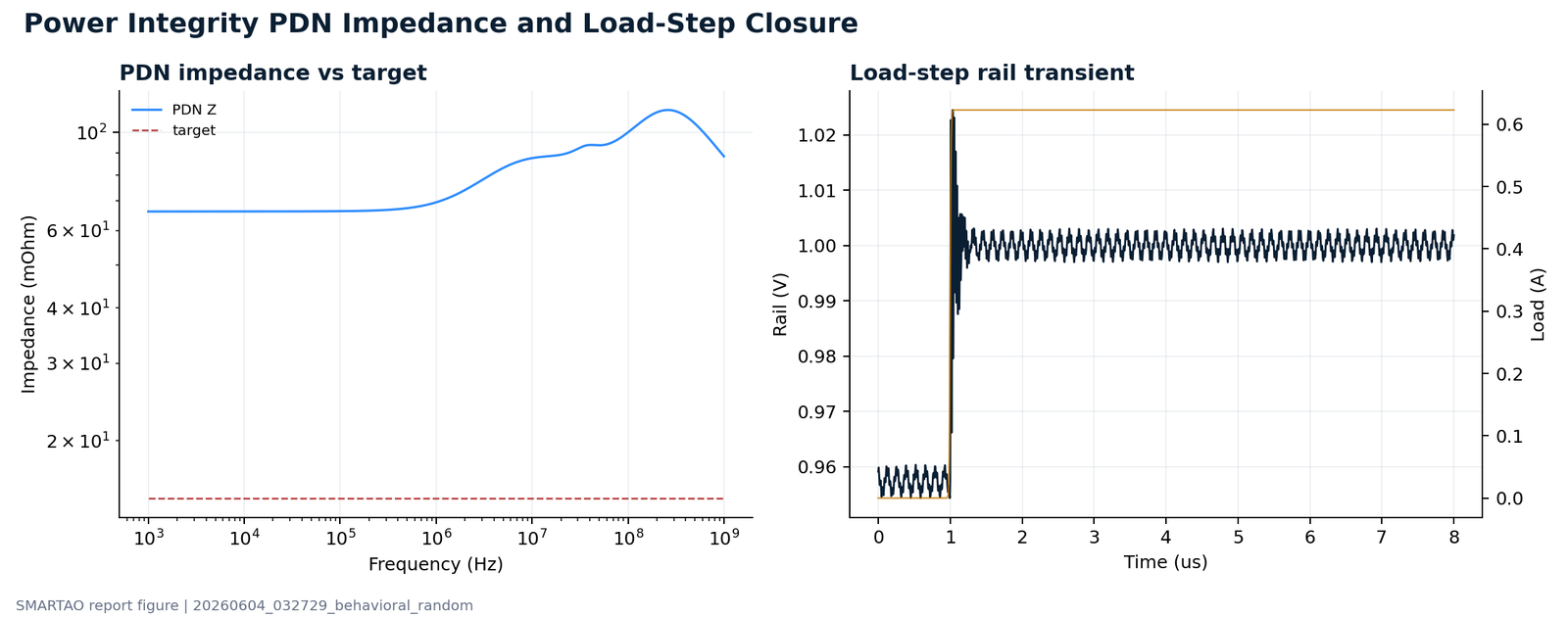
Target-impedance comparison, load-step rail transient, droop, ripple, and decap-driven PDN tradeoffs.
SMARTAO turns reusable testbenches, Cadence-oriented simulation, metric extraction, optimization, behavioral/RNM modeling, and report generation into one practical engineering loop.
The current library is organized around reusable RF/analog module classes and customer-owned design instances. In a Cadence-based deployment, the same infrastructure supports circuit-level and system-level test execution, optimization loops, behavioral/RNM modeling, and model-vs-schematic or model-vs-system validation. Developer-provided platform files and customer-generated workspaces are separated so upgrades do not overwrite private projects.
Module-aware testbench packages include DUT wrapper contracts, variableized parameters, stimuli, node maps, OCEAN/MDL measurement hooks, and SKILL schematic-generation entry points.
Optimization reads normalized metrics.txt outputs, compares candidates, handles PVT/MC validation, and can write optimized variables back into Cadence-oriented collateral.
Behavioral, RNM/EEnet, and coarse/fine model flows support faster exploration, schematic equivalence checks, and reusable model calibration.
Registered preprocessors and postprocessors cover supply ripple, jittered clocks, PAM4, modulation, ADC FFT, PLL phase noise, spurs, jitter, RF metrics, and SerDes DSP views.
A design intent can own multiple PDK-specific implementations. Each implementation is optimized and validated under its own PDK profile rather than pretending one schematic is portable.
Customers can add private design instances, architectures, and data locally. SMARTAO platform upgrades remain separate from customer-internal IP knowledge.
SMARTAO is not just a module list. It provides repeatable flows for RF/mmWave, power management, data conversion, high-speed IO, clocking, passive/EM, sensors, automotive, wireless, radar, SATCOM, and Bluetooth-style system scenarios.
Reusable module classes, candidate architectures, and project-specific design instances are stored separately. A 1 V LDO, a 2 V LDO, and several LNA or SerDes front-end architectures can be optimized independently or compared in one candidate run without overwriting each other.
Normal runs can produce report-ready figures, not only scalar metrics. The examples below are drawn from current SMARTAO demos and show closed-loop coverage across power integrity, data converters, RNM/EEnet model validation, passive RLCK fitting, PLL noise, 112G SerDes, DC-DC conversion, optical PAM4, RF transceiver chains, memory PHY, FMCW radar, and mmWave array systems. Dual-comb/DCS material is intentionally left out of this public page.
Target-impedance comparison, load-step rail transient, droop, ripple, and decap-driven PDN tradeoffs.
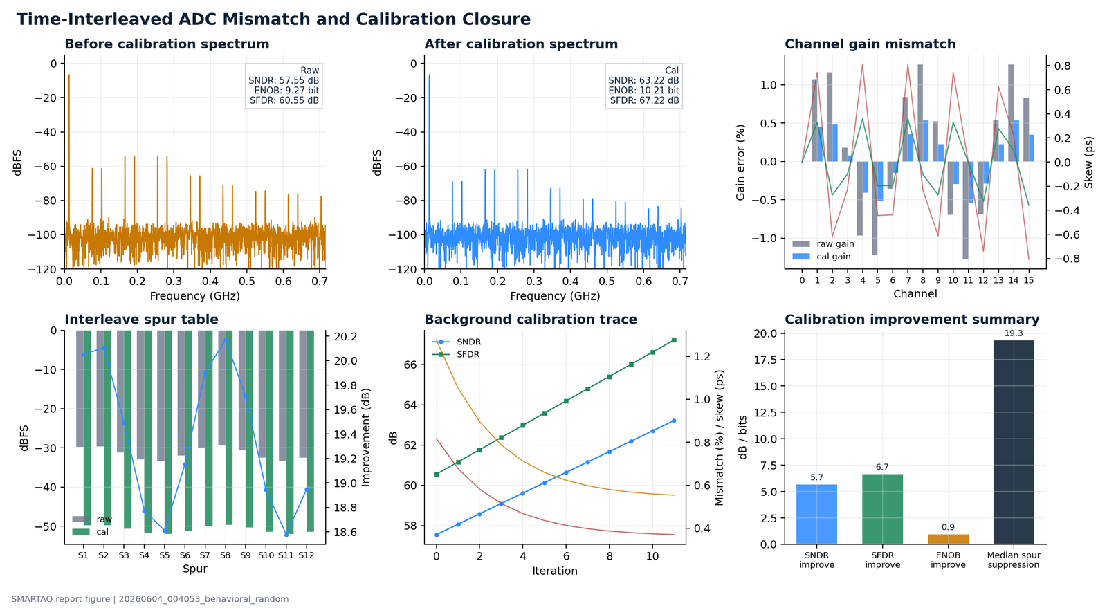
Raw versus calibrated spectrum, channel mismatch, interleave spur suppression, and background calibration trace.
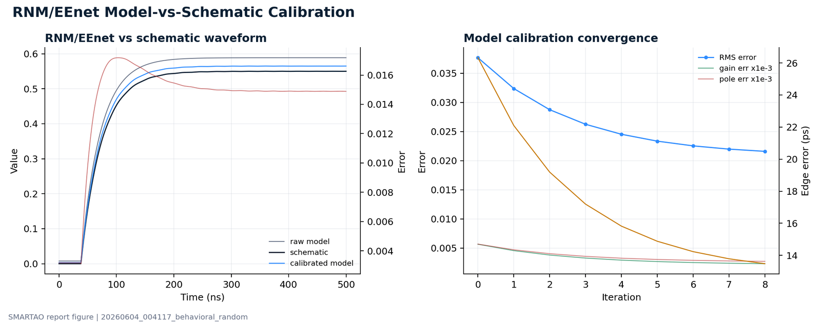
Raw model, calibrated model, schematic waveform, residual error, and calibration convergence in one view.
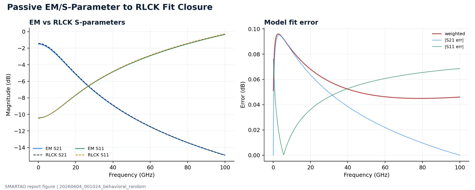
EM-like S-parameters overlaid with fitted RLCK model curves and frequency-dependent fitting error.
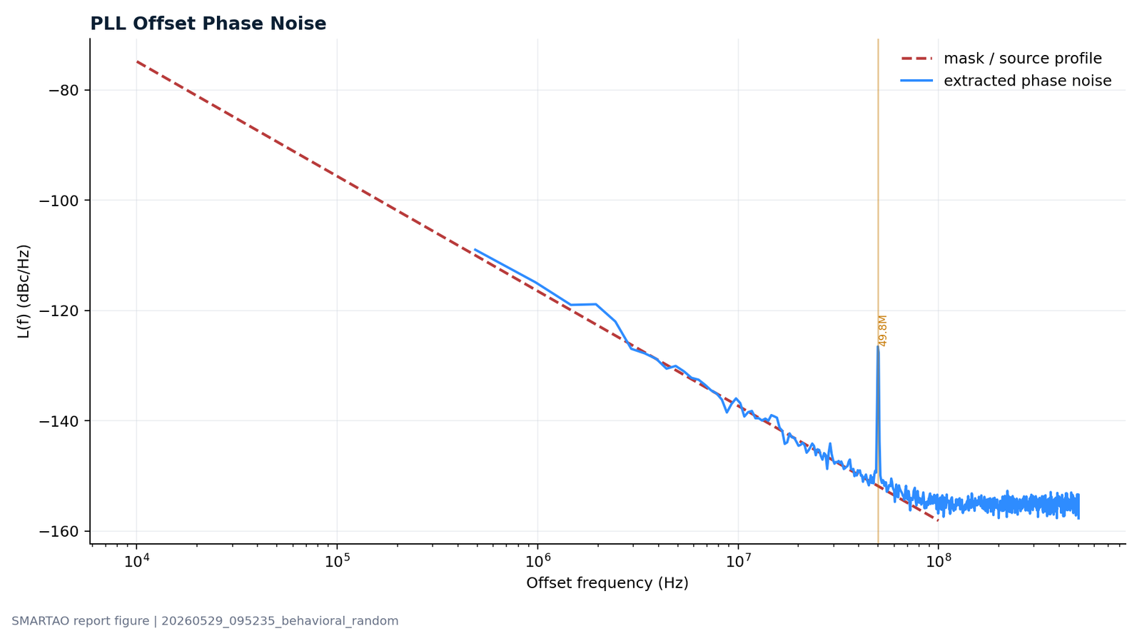
PSD, offset phase-noise mask, jitter, reference spur, and fractional-spur extraction from waveform data.
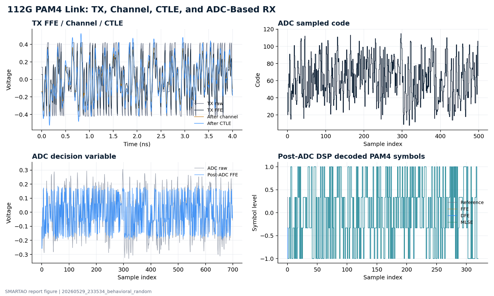
TX FFE, channel, CTLE, ADC samples, and post-ADC DSP decision variables in one view.
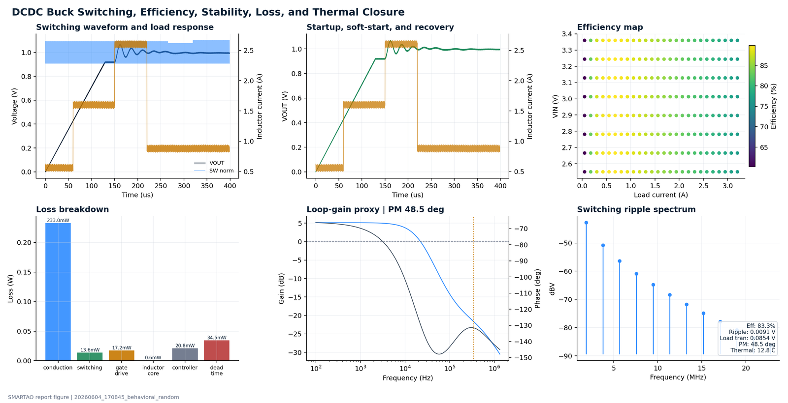
Switching waveform, startup, efficiency map, loop-gain proxy, ripple spectrum, loss breakdown, and thermal closure.
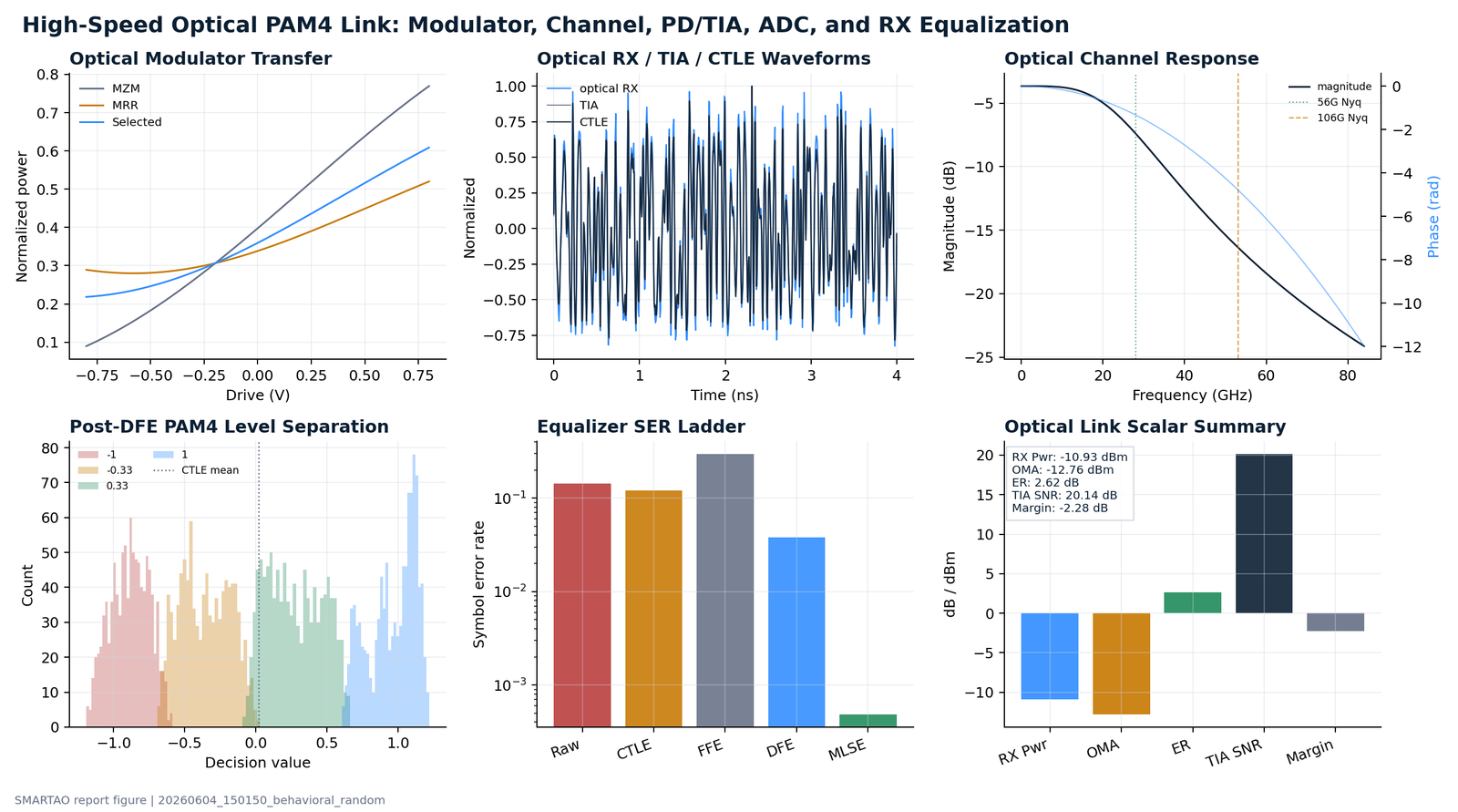
PAM4 stimulus, TX FFE, optical modulator/channel, PD/TIA, ADC, RX equalization, and link-quality metrics.
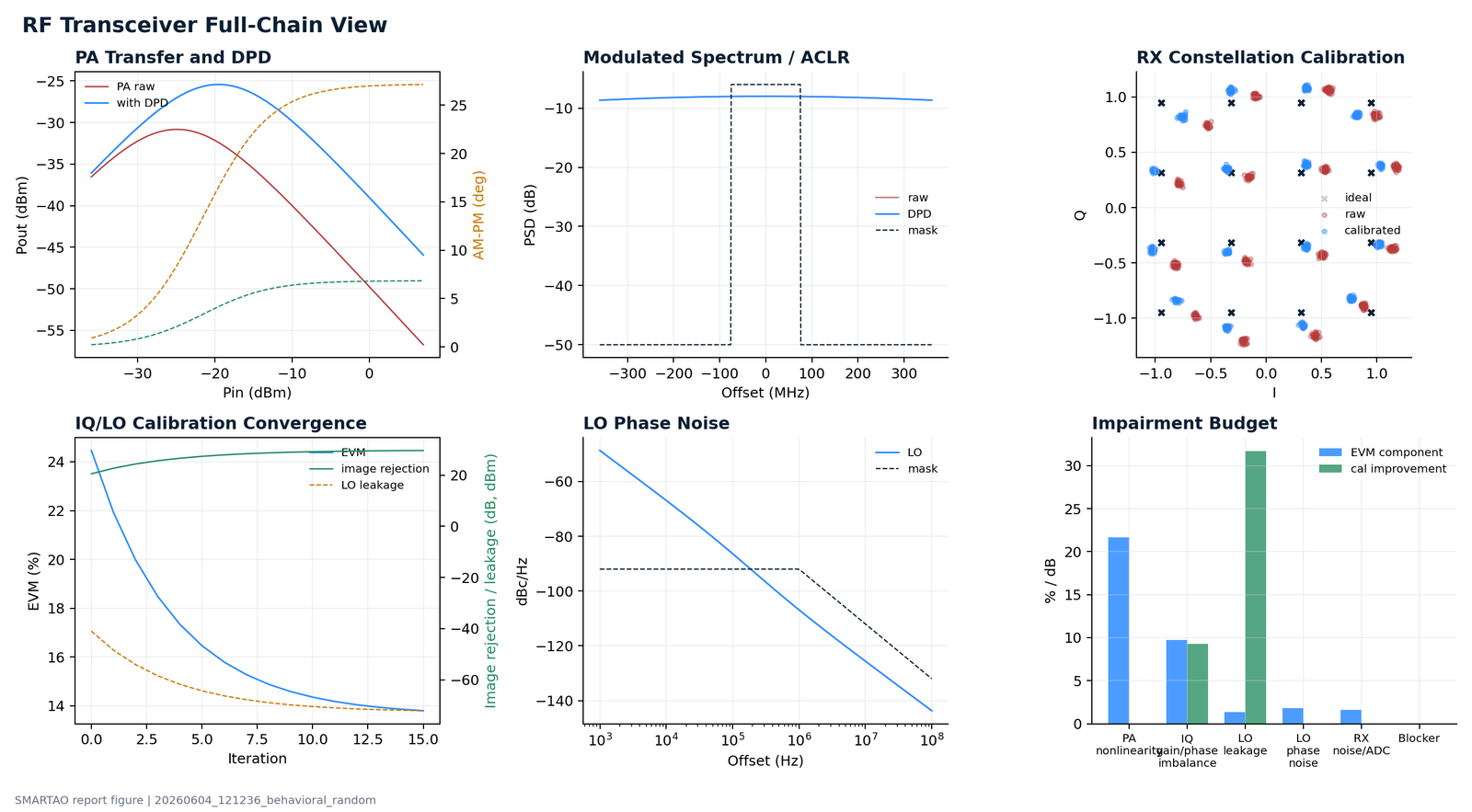
TX/RX impairment budget with DPD, PA nonlinearity, IQ imbalance, LO leakage, phase noise, EVM, ACLR, and calibration closure.
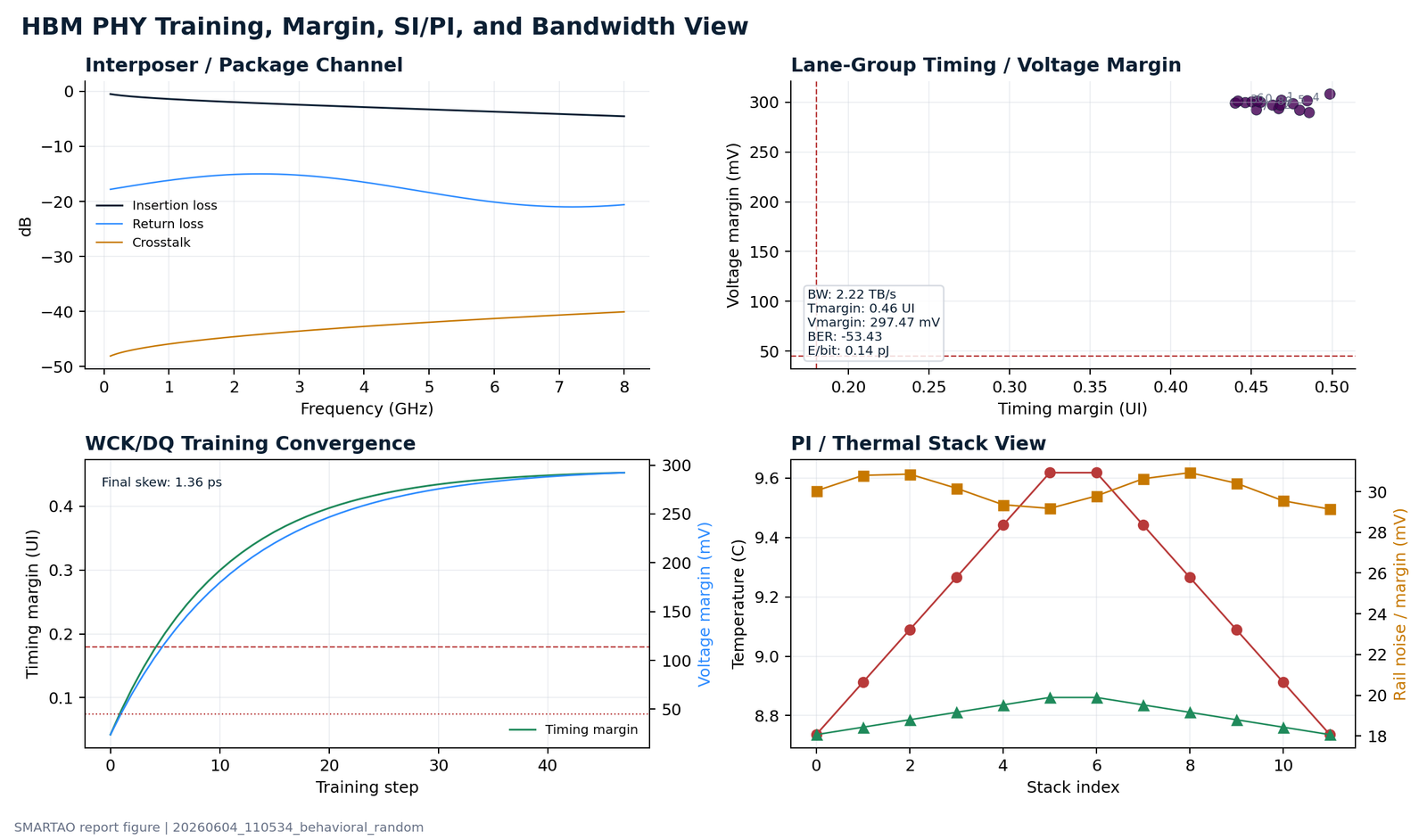
Wide-I/O memory PHY view with channel response, lane margin, training convergence, PI/thermal stress, bandwidth, and energy closure.
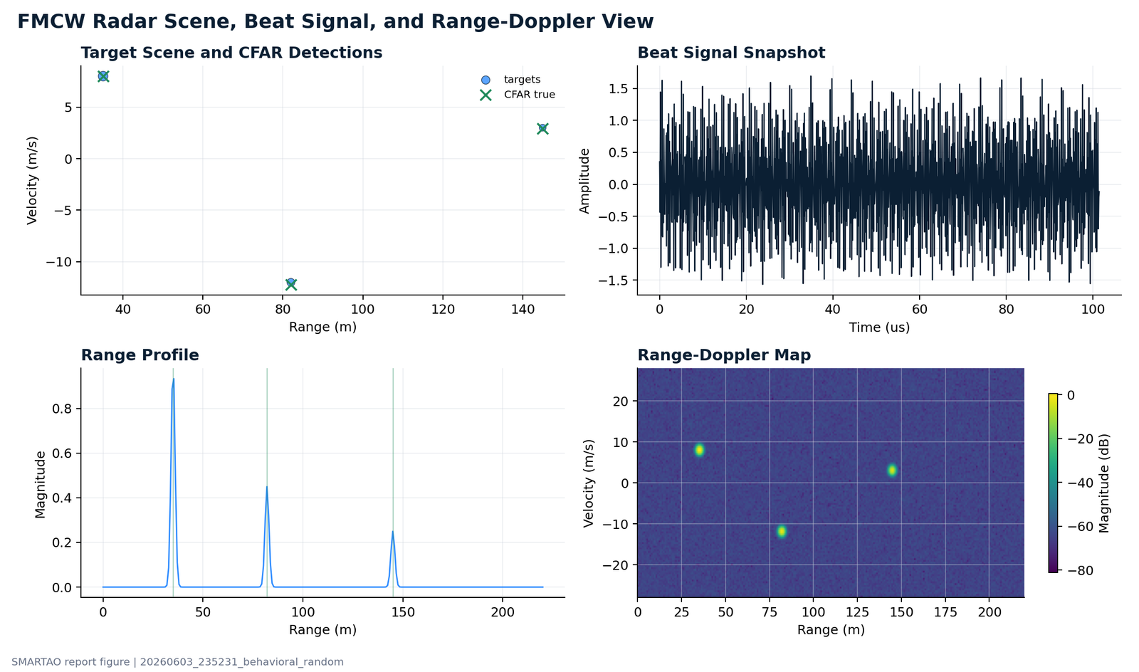
Chirp scene generation, beat waveform, range profile, range-Doppler map, detection view, and radar metric closure.
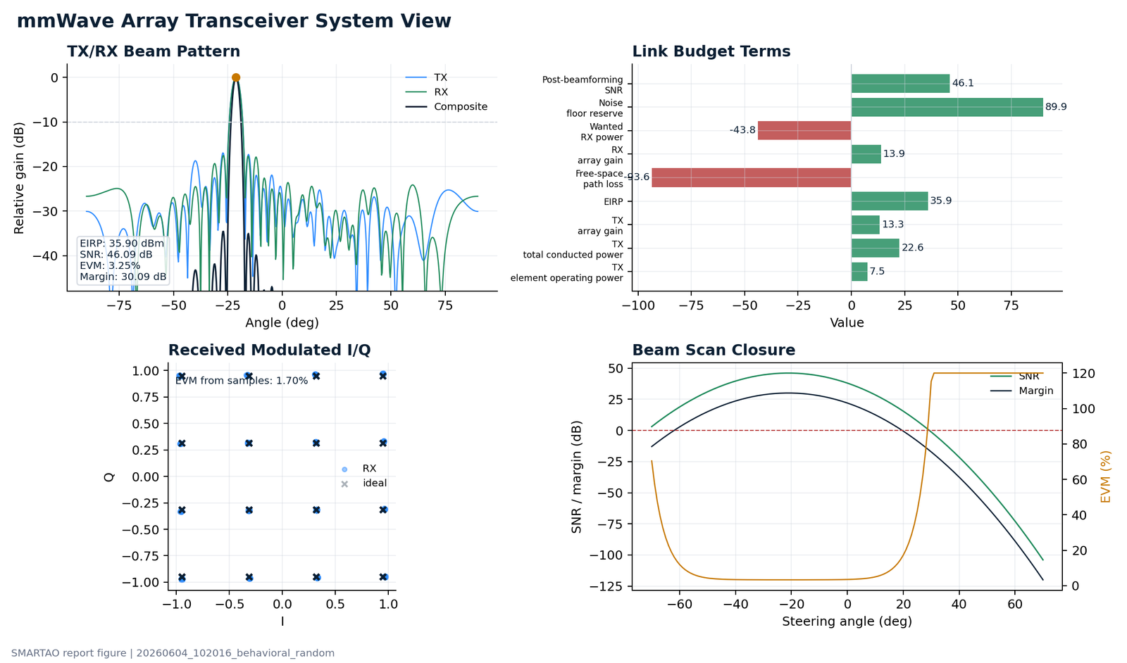
Beamforming, TX/RX link budget, blocker behavior, scan metrics, EVM, sidelobe, and array-calibration style closure.
The strongest early use cases are blocks where the engineering loop is expensive, testbenches are reusable, and scalar specs do not tell the whole story.
LDOs, digital LDOs, DC-DC converters, battery paths, UVLO/POR, power integrity, and automotive PMIC scenarios.
Integer/fractional PLLs, ADPLL/DCO, VCOs, DTC/TDC, LO distribution, jitter injection, phase-noise and spur workflows.
112G SerDes, ADC-based receivers, TX FFE, CTLE, FFE/DFE/CDR, MLSE/Viterbi post-processing, and PAM4 stimulus generation.
LNA, PA, mixers, RF switches, phase shifters, front-end modules, mmWave phased arrays, radar, WiFi/cellular, and SATCOM-oriented tests.
SAR, sigma-delta, time-interleaved, pipelined, hybrid ADCs, DACs, sample-and-hold, code-density and FFT post-processing.
Inductors, transformers, baluns, transmission lines, couplers, filters, RLCK fitting, layout SKILL seeds, and EM-to-circuit closure.
The first customer-facing step should be a focused pilot around one real circuit block, one existing Cadence testbench, or one high-value system scenario that needs reusable testing, optimization, and modeling.
Select one block, define specs, review the existing Cadence testbench, and bind nodes/variables.
Connect metrics, preprocess/postprocess profiles, and initial optimization variables.
Run candidate optimization, PVT/MC validation, visual reports, and model-calibration experiments.
Deliver a reusable flow package, results review, next-block plan, and licensing path.
Customer designs, PDK paths, simulation data, and learned project knowledge remain in the customer workspace by default. Platform upgrades and customer private instances are deliberately separated.
SMART = intelligence, efficiency, automation. TAO = method, engineering path, tools, and discipline. The brand stands for practical automation that guides complex semiconductor design toward verifiable and reusable results.
Short posts can turn SMARTAO from a private tool into a visible technical point of view without exposing source code or customer IP.
Analog optimization is usually limited by how repeatable the measurement loop is, not by the optimizer itself.
Analog IP optimization is not limited by the optimizer. It is usually limited by how repeatable the measurement loop is.
For many analog and RF blocks, the real engineering effort sits in the testbench: biasing the DUT correctly, applying realistic stimuli, defining corners, extracting meaningful metrics, and making sure every candidate is evaluated in the same way. Without reusable testbench infrastructure, every optimization run becomes a fragile one-off experiment.
A good reusable testbench standardizes the interface between design variables, simulation setup, and measured results. The optimizer should not need to understand every schematic detail. It should see a clean parameter set and a consistent metrics file.
It also captures engineering judgment. The right load transient for an LDO, the right two-tone setup for an LNA, the right jitter and channel condition for a SerDes receiver, or the right FFT window for an ADC are all part of the design knowledge. Reusable testbenches preserve that knowledge.
Most importantly, reusable testbenches make results comparable. Architecture A, architecture B, different PDK corners, and later design revisions can all be evaluated through the same measurement contract. That is what turns optimization from trying many simulations into a disciplined design flow.
A single eye diagram can show whether one case looks open, but it cannot explain where the link margin came from.
An eye diagram is useful, but for 112G SerDes it is not enough.
At 112G PAM4, the link is a chain of tightly coupled impairments: TX FFE tap settings, package and channel loss, CTLE peaking, ADC resolution, clock jitter, CDR behavior, FFE/DFE adaptation, and sometimes MLSE or other sequence detection. A clean-looking eye at one point in the chain may not tell you why the link works, where the margin comes from, or what will fail across corners.
A stronger optimization flow needs stage-aware metrics. Before the receiver, we need channel insertion loss, return loss, crosstalk, and TX pre-emphasis. Inside the receiver, we need CTLE response, ADC input range, quantization noise, timing margin, and equalizer convergence. After detection, we need SER or BER estimates, error distribution, jitter tolerance, and adaptation stability.
It also needs realistic stimuli. PAM4 symbols, PRBS patterns, jitter injection, bandwidth-limited channels, and stressed channel conditions reveal problems that a simple waveform snapshot can hide.
A single eye diagram answers, does this case look open? A serious 112G SerDes optimization flow answers why it is open, how much margin exists, and which knobs actually created that margin.
AI can assist the workflow while schematics, PDK data, layouts, and proprietary waveforms remain inside the company environment.
RF and analog teams can benefit from AI without exposing schematics, PDK data, or proprietary design details.
The key is to keep AI close to the workflow, but far from confidential implementation data. Instead of sending full schematics or layouts to an external model, teams can expose structured, limited information: block type, target specs, allowed variables, simulation status, metric names, and anonymized failure modes.
AI is especially useful around the design loop. It can help generate test plans, suggest likely measurements, organize optimization variables, explain failed simulations, compare candidate results, and draft reports. These tasks need engineering context, but not the full circuit.
A safe architecture separates three layers: a private layer for schematics, PDK files, simulation waveforms, extracted views, and customer-specific IP; a structured interface layer for sanitized specs, corners, variable ranges, metric outputs, logs, and workflow states; and an automation layer that applies approved actions locally.
For RF/analog design, the most practical use of AI may not be generating a complete circuit. It may be helping engineers run better experiments, reuse knowledge, diagnose issues faster, and turn simulation data into decisions while keeping the real IP safely inside the design environment.
SMARTAO is suitable for pilot evaluations, internal IP development, design automation partnerships, and investor/customer discussions around RF/analog IC automation.
Founder: Yusheng (Boris) Chen
RF/Analog and mixed-signal IC designer building AI-assisted automation infrastructure for reusable testbenches, simulation-driven optimization, behavioral modeling, and system-level validation.
RF/Analog IP Automation · Simulation · Optimization · Modeling